(주)코셈은 나노측정기술(Nano-Metrology) 전문회사로서 한국표준과학연구원이 6~7년에 걸쳐 개발한 전자현미경 기술을 기반으로 2007년도에 설립되었습니다. 코셈은 대덕연구단지의 기술과 대덕R&D특구펀드 및 산업은행의 자금으로 세워진 대덕특구의 전형적인 기술사업화 기업입니다.
(주)코셈은 nano scale의 측정기술(Nano-Metrology) 중에서 가장 널리 활용되고 있는 platform 기술인 주사전자현미경(SEM; scanning electron microscope)을 개발•생산하고 있으며, 21세기 산업의 지형을 변화시키고 있는 나노 융합기술의 partner로서 최선을 다하고 있습니다
SEM은 미세 구조물의 형상과 구성 성분들의 조성을 정량, 정성적으로 측정할 수 있는 정밀기기로서 반도체/디스플레이, 나노소재/소자, 나노바이오 등 융•복합 산업은 물론 화학, 생명과학, 재료과학 등 기초과학의 발전을 위해 필수적인 도구이자 기술혁신을 위한 인프라입니다.
㈜코셈은 2008년 보급형 SEM을 상용화하여 국내시장에서 적극적인 마케팅을 전개하고 있으며, 2009년부터 미국, 일본, 유럽 등 글로벌 마케팅에 본격적으로 착수하고 있습니다.
측정기술은 모든 과학기술의 기반기술로서 우수한 측정 도구 없이는 창의적 기술개발은 불가능합니다. ㈜코셈은 국내 나노 융합산업의 Partner로서 나노기술 강국 대한민국의 미래를 위해 최선의 노력을 다할 것이며, 세계시장에서 전자현미경 global leader로 거듭나기 위해 매진할 것을 다짐합니다.
■ (주)코셈의 Brief History
2009년 12월 미국 EVEX와 OEM 공급 계약. Demo용 CX-100 선적
6월 ISO 9001/14001 인증 획득
2008년 11월 대덕특구과제/기술혁신과제 사업자 선정
6월 보급형 SEM(모델 CX-100S) 시판
5월 중소기업 선도기술과제 선정(2년간)
4월 신기술인증서(NET) 획득
1월 벤처기업 확인
2007년 10월 기업부설연구소 설립
6월 회사 설립, 표준과학연구원과 SEM 기술이전 계약
과학기술부 대덕R&D특구펀드(과기부+산업은행+대전시 출자) 투자유치
■ 표준과학연구원의 SEM 개발연혁
1996 반도체 장비•소재 국산화 기획사업추진 (반도체산업협회 주관)
1997 러시아, 우크라이나 등 구 동구권의 전자현미경기술보유실태조사
2000 일본의 퇴역기술자에 기술지원요청à 거절당함
2001 자체 예산으로 개발/도면제작 (외국장비의 Reverse Engineering)
2003 아나로그형 SEM으로 50,000배 영상획득 성공
2004 과기부 나노핵심사업으로 전자현미경개발과제 착수à독자적인 디지탈회로, 고전압회로설계
2005 과기부 21C 프런티어사업으로 전자선 로광장비 개발사업 착수 à 로광 실험 성공 à 디지털 SEM 개발 성공
2010년 7월 15일 목요일
Ion Coater for SEM sample preparation

COXEM (http://www.coxem.com/) supplies a ion sputter coater, Model KIC-1A with stable ion current, with a simple manipulation and setting methods. It can produce uniform particle sizes and coating thickness.
Specification
· Rapid pumping, less than two minute
· Rapid pumping, less than two minute
· Fast operation with preset values
· Easy job setup
· Automatic vacuum control
· Automatic ventilation after coating
· Easy adjustment of sample height
· Target size: 50 mm (Gold / Platinum)
· Power: 220V/60Hz, 500W
· Ionization current: 1 ~ 7 mA
· Dimension: 380(W) x 250(D) x 330(H) mm
· Chamber size: 100 mm (Dia.)
· Rotary pump: 100 liter/min.
Contact : sem.jeong@gmail.com
COXEM, Pioneer in Electron Miscroscope
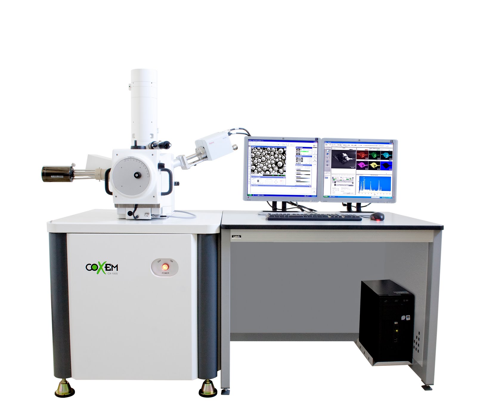
Scanning Electron Microscope, CX-100S
Versatile Tool to Access the Nano-World
The optical microscope is the most commonly used tool in surface metrology generally and it is widely used in educational programs, R&D and quality control. However, the optical microscope can not fulfill the growing demand for higher magnification due to its physical limitations. The CX-100S SEM is a powerful tool for surface characterization which produces high quality images with nano-scale resolution. Its software is using the graphical user interface and based-on and Microsoft Windows XP or 7. Company website: www.coxem.com
Indispensable Tool for Materials Analysis
CX-100S is an indispensable tool for various application areas in materials analysis. It has a high resolution (3.5 nm at 30 kV acceleration voltage and SE detector) and a high magnification imaging for surface morphology in the nanoscale. The clean imaging is due to its long depth of focus.
User Friendly Operation
NanostationTM is the powerful software for the system control and image analysis for the CX-100S SEM. It is designed and based-on Microsoft Windows XP and adapted a user-friendly interface. NanostationTM allows for a customized toolbars for repeat job setup.
High Performance / Economic Grade
The CX-100S is a state-of-the-art SEM with a veriety of detector choices, the user can enjoy a high performance SEM at an economic price.
Rapid Analysis
The CX-100S uses an oil-free turbo molecular pump. The speed of the pump will allow for imaging in under five minutes up to 10-6 torr.
Diverse Range of Applications
CX-100S provides the best imaging solution over a wide spectrum of samples from bio-molecules to metal samples. The CX-100S can be equipped with additional detectors like EDS and/or BSE and can run both simultaneously.
Contact: sem.jeong@gmail.com
피드 구독하기:
글 (Atom)