원문 : http://kin.naver.com/open100/detail.nhn?d1id=11&dirId=110404&docId=1332907
네이버 지식인에 직접 작성한 글입니다.
우리가 눈으로 볼 수 있는 빛을 가시광선이라 하며, 물체가 색을 나타내는 것 역시 가시광선 영역의 빛이 물체에서 반사되기 때문입니다. 전자기파의 일종인 빛 중에서 우리가 볼 수 있는 영역은 파장이 400 nm에서 950 nm 정도가 되겠죠. 적외선 이상의 장파장과 단파장인 자외선 등은 보이지 않습니다.
일반 현미경(광학현미경)은 시편에 빛을 반사 또는 투과시켜 눈으로 관찰하거나 CCD 카메라를 달아서 모니터로 관찰할 수 있습니다. 그러나 전자현미경은 빛이 아닌 전자빔을 이용합니다. 가속된 전자빔이 시편에 충돌할 때 시료 표면에서 방출되는 이차전자를 포집하여 표면의 형상을 관찰하는 것이죠.
전자빔으로 표면을 스캔하여 각 point에서 방출되는 이차전자의 세기를 모니터 화면상에 밝기(명암)으로 표시하게 됩니다. 따라서 우리가 볼 수 있는 전자현미경 영상은 흑백일 수 밖에 없습니다. 또한 눈으로 직접 관찰은 불가능하고, 전기적 신호(아날로그 신호)를 디지털로 변환시킨 후 PC를 거쳐 모니터를 통해서 관찰할 수 있습니다.
간혹 우리가 볼 수 있는 칼라 이미지는 실제 영상이 아닌 이미 얻어진 이미지를 포토샵과 같은 프로그램을 이용하여 인위적으로 색을 덧쒸운 것입니다.
이러한 한계에도 불구하고 전자현미경을 많이 사용하는 이유는 10만배 이상의 고배율까지 측정할 수 있기 때문이죠. 광학현미경은 아무리 성능이 뛰어나고 비싼 제품을 쓰더라도 2000배 이상은 관찰할 수 없습니다.
쉽게 말해서 광학현미경이 마이크로 카메라라고 한다면 전자현미경은 나노 카메라로 부를 수 있겠죠.
2010년 9월 1일 수요일
주사전자현미경 개요
원문 : http://coxem.kr/110081081517
1. 전자현미경의 기본개념
(1) 전자현미경이란?
최근 정보기기들의 극소화 추세 뿐만 아니라 첨단 소재 분야에서도 극미세 기술의 산업화로 인해미세구조물 또는 재료의 표면형상에 대한 정보가 절실히 요구되고 있다. 특히, 1990년대 후반부터 전세계적으로 나노연구가 활발해지면서 나노물질의 구조와 특성을 규명하기 위한 다양한 연구들이 진행되고 있으며, 전자현미경은 중요한 축을 담당하고 있다.
전자현미경(Electron Microscope)은 광학현미경(Light Microscope)에서 사용하는 가시광선(visible rays) 대신 전자선(electron beam)을, 또한 유리렌즈(glass lens) 대신에 전자렌즈(electron lens)를 사용하여 물체의 확대상을 만드는 장치를 말한다.
1920년대에 기존 현미경의 한계를 극복할 수 있는 새로운 미세 관찰 기술이 요구되었으며, 전자의 자계에 의한 렌즈 작용을 이론화하여 현미경의 새로운 광원으로 전자를 사용하게 되었는데 이를 계기로 새로운 현미경의 이름을 전자현미경이라 부르게 되었다. 전자현미경은 전자에 대한 렌즈작용을 코일에 흐르는 전류를 변환시킴으로써 자계(magnetic field)를 사용하여 전자의 이동 경로를 휘게 하여 마치 볼록렌즈가 빛을 집속하듯 전자를 모아주는 것과 유사하다.
전자현미경은 광선 대신에 전자 빔을 사용하기 때문에 현미경의 내부는 진공상태여야 한다. 전자는 공기와 충돌하면 에너지가 소실되거나 굴절되는 등 원하는 대로 제어하기 어렵기 때문이다. 전자현미경은 표본과 대물렌즈와 렌즈 사이의 거리는 일정하지만 중간렌즈와 투영렌즈의 코일에 통하는 전류의 세기에 의해 배율이 결정되며 상의 초점은 대물렌즈의 코일에 흐르는 전류에 의해 조절된다.
광학현미경은 실제의 상을 볼 수 있지만 전자현미경은 형광판이나 사진판을 통해 상을 볼 수 있다. 광학현미경은 표본의 빛을 흡수/반사함으로써 상이 형성되는 반면, 전자현미경에서는 전자선이 시료의 표면에 충돌하면서 발생하는 이차 전자, 산란전자,투과전자, X-Ray 등을 측정하여 표면의 형태를 영상으로 나타낸다.
(2) 전자현미경으로 얻을 수 있는 정보
전자현미경으로 재료의 표면형상, 적층 결함, 계면 등을 직접 관찰함에 따라 이들이 재료의 여러 성질들에 미치는 영향을 정확히 규명할 수 있다. 전자회절로써 결정의 결자상수와 대칭성 등을 규명할 수 있고, 분석전자현미경으로 원자의 종류와 양을 분석할 수 있다. 그리고 고 분해능 전자현미경으로 원자의 배열을 관찰할 수 있다. 이들 전자현미경 기술을 이용하면 원자의 종류와 위치를 원자 규모로 규명할 수 있고 따라서 이들이 재료의 성질에 미치는 영향을 규명하여 새로운 재료의 개발에 이용할 수 있다.
전자현미경으로 얻을 수 있는 정보는 크게 다음과 같다.
∙ Topography (물체의 표면의 형상을 관찰)
물체의 미세구조와 hardness, reflectivity 등의 물성과 연관성을 규명할 수 있다.
∙ Morphology (물체를 구성하는 입자들의 형상과 크기 관찰)
ductility, strength, reactivity 등의 물성과의 직접적인 관계를 알 수 있다.
∙ Composition (물체를 구성하는 원소와 화합물의 종류 및 상대적인 양을 분석)
분광학에 의한 전자와 시편이 상호 작용하여 생기는 X-선이나 전자를 분석하여 시편 내에 존재하는 원자의 종류와 양을 알아내는 방법으로 에너지 분산 X-선 분광학과 전자 에너지 손실 분광이 있다. 즉, 분광학을 이용한 재료표면의 원소의 종류와 양은 같은 화학적 조성 정보를 제공한다. 녹는점, 반응성, 경도 등 재료물성과 조성과의 관계를 알 수 있다.
∙ Crystallography (재료 내 원자들의 배열상태 분석)
재료의 여러 성질들은 미세 구조, 즉 원자의 종류와 위치에 큰 영향을 받는다. 전자와 시편 내의 원자 간의 간섭을 이용하여 원자의 위치 및 배열에 대한 정보를 얻는 것이다. 회절 패턴을 이용한 결정 구조정보와 같은 역공간의 정보를 제공한다. conductivity, electrical properties, strength 등의 재료고유 물성과 원자배열과의 관계 연구할 수 있다.
(3) 전자현미경의 특징
전자현미경은 높은 에너지의 전자빔을 이용하여 전자가 시편과 충돌할 때 발생하는 이차전자, 반사전자, X-선 등을 검출하여 확대상을 촬영하는 장치이다.
(주사)전자현미경의 특징을 살펴보면 첫째, 분해능이 높기 때문에 고배율로 물체를 관찰할 수 있다. 열방사형 텅스턴 필라멘트 방식의 SEM은 10만배 이상(분해능: 3~5 nm), 전계방사형 SEM(FE-SEM)은 최대 100만배(분해능: 0.5~2 nm)까지 확대상을 얻을 수 있다.
둘째, SEM은 고배율 뿐 아니라 10~100배의 저배율 관찰에도 사용할 수 있다. SEM은 렌즈를 교환하지 않고 단지 코일에 흐르는 전류를 변화시켜 배율을 조절할 수 있기 때문이다. 일반적으로 저배율에서 넓은 면적을 관찰한 후 관심 있는 미세영역을 고배율로 관찰한다.
셋째, 전자현미경은 광학현미경과 달리 피사계 심도가 대단히 깊다. 피사계 심도란 관찰 대상물의 확대영상에서 초점이 맞는 깊이 범위를 말한다. 디지털 카메라와 전문가용 고성능 카메라의 차이를 비교해보면 쉽게 이해할 수 있다. <그림2>은 광학현미경과 전자현미경으로 측정한 영상으로서 SEM 영상은 이차원 데이터임에도 불구하고 마치 3차원 이미지와 유사하여 물체를 훨씬 정확하게 관찰할 수 있다. 따라서 SEM은 요철이 심한 파단면의 관찰이나 표면조도가 큰 시료를 관찰하는데 매우 유리하다.
넷째, 최근 SEM은 디지털 영상을 제공하기 때문에 영상의 저장은 물론 영상에 대한 다양한 분석이 가능하다. 과거에는 소형CRT 모니터를 통해서 영상을 볼 수 있던 때와 차원이 다른 다양한 기능을 제공한다. 보는 것이 믿는 것이란 말이 있듯이 R&D분야는 물론 산업체의 품질관리 성적서에서 미세구조물에 대한 영상자료를 제시하는 것 보다 더 확실한 방법은 없을 것이다.
다섯째, 다양한 검출기 및 주변기기를 장착하여 응용분야를 확장할 수 있다. 대표적인 검출기는 후방산란전자를 측정할 수 있는 BSE(back Scattered Electron) 검출기와 특성 X선을 검출할 수 있는 EDS(energy dispersive X-ray spectroscope)와WDS(wavelength dispersive X-ray spectroscope) 검출기가 대표적이다. 특히, X선 분광분석법은 짧은 시간에 미세영역의 구성성분을 분석할 수 있기 때문에 이차전자 검출기와 함께 필수적 검출기법이 되고 있는 추세이다.
전자현미경의 단점이라면 우선, 고전압(0.5~30 kV)을 사용하여 가속전자를 발생시키므로 여러 가지 복잡한 장치가 요구되며,전자빔을 이용하기 때문에 진공(10-5 torr 이하)이 필수적이다. 이 두 가지 요소(고전압과 진공기술)로 인해 전자현미경은 크고 복잡하며 가격 또한 비쌀 수 밖에 없다.
한편, 전자현미경에서 부도체 시료의 관찰시 전자빔의 전자가 시료에 축적되어 궁극적으로 전자빔을 밀어내는 역할을 하게 되므로 이미지가 왜곡 될 수 있다. 이 때문에 부도체 시료의 경우 표면을 Au 또는 Pt 등의 전도체로 코팅하는 것이 바람직하다.
이와 같은 단점은 생체시료를 측정할 때 많은 한계로 나타나게 된다. 그러나 최근에는 저진공 SEM(가변 진공 SEM또는Environmental SEM이라고도 함), Cryo-SEM 및 Charge Redution 기술 등이 개발되어 SEM의 활용분야가 확장되고 있는 추세이다.
2010년 7월 15일 목요일
나노융합기술의 파트너, (주)코셈
(주)코셈은 나노측정기술(Nano-Metrology) 전문회사로서 한국표준과학연구원이 6~7년에 걸쳐 개발한 전자현미경 기술을 기반으로 2007년도에 설립되었습니다. 코셈은 대덕연구단지의 기술과 대덕R&D특구펀드 및 산업은행의 자금으로 세워진 대덕특구의 전형적인 기술사업화 기업입니다.
(주)코셈은 nano scale의 측정기술(Nano-Metrology) 중에서 가장 널리 활용되고 있는 platform 기술인 주사전자현미경(SEM; scanning electron microscope)을 개발•생산하고 있으며, 21세기 산업의 지형을 변화시키고 있는 나노 융합기술의 partner로서 최선을 다하고 있습니다
SEM은 미세 구조물의 형상과 구성 성분들의 조성을 정량, 정성적으로 측정할 수 있는 정밀기기로서 반도체/디스플레이, 나노소재/소자, 나노바이오 등 융•복합 산업은 물론 화학, 생명과학, 재료과학 등 기초과학의 발전을 위해 필수적인 도구이자 기술혁신을 위한 인프라입니다.
㈜코셈은 2008년 보급형 SEM을 상용화하여 국내시장에서 적극적인 마케팅을 전개하고 있으며, 2009년부터 미국, 일본, 유럽 등 글로벌 마케팅에 본격적으로 착수하고 있습니다.
측정기술은 모든 과학기술의 기반기술로서 우수한 측정 도구 없이는 창의적 기술개발은 불가능합니다. ㈜코셈은 국내 나노 융합산업의 Partner로서 나노기술 강국 대한민국의 미래를 위해 최선의 노력을 다할 것이며, 세계시장에서 전자현미경 global leader로 거듭나기 위해 매진할 것을 다짐합니다.
■ (주)코셈의 Brief History
2009년 12월 미국 EVEX와 OEM 공급 계약. Demo용 CX-100 선적
6월 ISO 9001/14001 인증 획득
2008년 11월 대덕특구과제/기술혁신과제 사업자 선정
6월 보급형 SEM(모델 CX-100S) 시판
5월 중소기업 선도기술과제 선정(2년간)
4월 신기술인증서(NET) 획득
1월 벤처기업 확인
2007년 10월 기업부설연구소 설립
6월 회사 설립, 표준과학연구원과 SEM 기술이전 계약
과학기술부 대덕R&D특구펀드(과기부+산업은행+대전시 출자) 투자유치
■ 표준과학연구원의 SEM 개발연혁
1996 반도체 장비•소재 국산화 기획사업추진 (반도체산업협회 주관)
1997 러시아, 우크라이나 등 구 동구권의 전자현미경기술보유실태조사
2000 일본의 퇴역기술자에 기술지원요청à 거절당함
2001 자체 예산으로 개발/도면제작 (외국장비의 Reverse Engineering)
2003 아나로그형 SEM으로 50,000배 영상획득 성공
2004 과기부 나노핵심사업으로 전자현미경개발과제 착수à독자적인 디지탈회로, 고전압회로설계
2005 과기부 21C 프런티어사업으로 전자선 로광장비 개발사업 착수 à 로광 실험 성공 à 디지털 SEM 개발 성공
Laser Scanning Confocal Microscope

Indispensable Tool for Materials Analysis
Confocal Laser Scanning Microscopy (CLSM) is a optical 3-dimensional (3D) surface profilerwith a high-resolution. With a high numerical aperture objective lens (up to 0.95) and a shorterwavelength laser provide a high-resolution imaging along both the optical and transversedirection. A confocal pinhole also improves the imaging quality by rejecting the noise outsidethe focal point. Real time imaging is achieved by a fast scanning module and a signal processing algorithm. It takes less than 1 second to get the 3D surface profile of the sample.CLSM is a non-destructive high-resolution optical 3D surface profiler for the micro-structure. It is an ideal solution to measure and inspect the semiconductor wafers, FPD products, MEMS devices, glass surfaces, and material surfaces.
Confocal Laser Scanning Microscopy (CLSM) is a optical 3-dimensional (3D) surface profilerwith a high-resolution. With a high numerical aperture objective lens (up to 0.95) and a shorterwavelength laser provide a high-resolution imaging along both the optical and transversedirection. A confocal pinhole also improves the imaging quality by rejecting the noise outsidethe focal point. Real time imaging is achieved by a fast scanning module and a signal processing algorithm. It takes less than 1 second to get the 3D surface profile of the sample.CLSM is a non-destructive high-resolution optical 3D surface profiler for the micro-structure. It is an ideal solution to measure and inspect the semiconductor wafers, FPD products, MEMS devices, glass surfaces, and material surfaces.
The height measuring ability comes from the confocal setup of a source, a sample, and a detector. When the sample is located in the focal plane of the objective lens, the light reflected at the surface of the sample is focused at the confocal aperture thus the photodetector collects the signal from the sample. However the sample is placed in the out-of-focus position, the light signal is rejected by the confocl aperture. Thus only the in-focus signal is collected by the photo detector. It gives the optical sectioning ability to the CLSM. To get the 3D surface profile of the sample, optical sections are collected through the z-axis. Due to the confocal aperture, the light intensity is maximum when the sample is placed in the focal plane.
Maximum intensity is detected at the focal plane. The intensity decreases when the sample is away from the focal plane. To find the maximum intensity precisely, multi-points near the maximum position are used for the curve fitting. This provides high repeatability onmeasuring the height. The height is calculated by the curve fitting at every pixel. This height map shows the surface profile of the sample.A CLSM has many applications in the industrial fields since it is fast, nondestructive, and reliable 3D surface profiler. It can measure 3D shape, step height and volume of the micro structures. The LCD panels, semiconductor wafers, MEMS devices, material surfaces, andeven transparent glass surfaces can be measured and inspected. Moreover, a CLSM iswidely used for the biological researches. With a fluorescent die it can get a clear image of biological specimens from its own nature. 3D structure and dynamics of the cells also can bemeasured. Since a CLSM can observe the tissues under the skin it is applied to skin cancerdetection. Recently, confocal endoscope system has been introduced for the sub-micron gastrointestinal examinations.
High-speed confocal 3D profiler
NS-3000 is a high-speed confocal laser scanning microscope for precise and reliable 3D measurement.A real time confocal zmicroscopic image is achieved by fast opticalscanning modules and signal processing algorithms. It is a promising solution to measure and inspect the microscopic 3D structures such as semiconductor wafers, FPDproducts, MEMS devices, glass substrates,and material surfaces.
NS-3000 is a high-speed confocal laser scanning microscope for precise and reliable 3D measurement.A real time confocal zmicroscopic image is achieved by fast opticalscanning modules and signal processing algorithms. It is a promising solution to measure and inspect the microscopic 3D structures such as semiconductor wafers, FPDproducts, MEMS devices, glass substrates,and material surfaces.
Major Features
High resolution nondestructive optical 3D measurement
- Real time confocal imaging- Various optical zoom
- Simultaneous brightfield and confocal imaging
- Automatic gain search with fine auto focus
- Inclination compensation - Easy analysis mode
- Precise and reliable high-speed height measurement
- Inspection of features through semi-transparent substrate
- No sample preparationApplications : Surface Measurement and Inspection NS-3000 is designed for the measurement of HEIGHT, WIDTH, ANGLE, AREA and VOLUME of micro and submicro structures such as- Semiconductor
- IC pattern, bump hight, defect inspection, CMP process
- FPD products
- LCD column spacer height, PDP rib height, coating inspection
- MEMS devices
- 3D profile of structure, surface roughness, MEMS pattern- Glass surfaces
- Thin film solar cell, laser patterning, scratch depth- Material Researches
- Tooling surface inspection, roughness, crack analysis.
contact: sem.jeong@gmail.com
Scanning Probe Microscope
About SPM
 High Speed and High Pixel Imaging
The hardware and software of SPM support high-speed imaging mode where the fast z-actuator such as integrated micro-actuator will be used. The maximum scan rate depends onthe scan size and number of pixel per image. It is possible to increase frame rate up to 1frame/s for the 256x256 pixel point. High speed imaging can be performed by an auxiliary fast digital feed-back loop which is implemented on our digital controller. Our fast DSP-baseddigital feedback can work up to 100 kHz bandwidth.
SPM covers the full range scanning probe microscopy techniques to investigate the surfaceproperties like as topography, electronic, magnetic characteristics from nanoscale to severaltens of micron. The state- of-the-art DSP-based fast digital controller provides not only mucheasy and flexible operational interface but also sufficient high speed/resolution imaging solution. Also, our system provides very versatile Ethernet-based remote control of the SPMinstrument. Advance nanolithography tool supports the very convenient interface as well asvarious probe-based writing techniques.
High Speed and High Pixel ImagingThe hardware and software of SPM support high-speed imaging mode where the fast z-actuator such as integrated micro-actuator will be used. The maximum scan rate depends onthe scan size and number of pixel per image. It is possible to increase frame rate up to 1frame/s for the 256x256 pixel point. High speed imaging can be performed by an auxiliary fast digital feed-back loop which is implemented on our digital controller. Our fast DSP-baseddigital feedback can work up to 100 kHz bandwidth.

· High Speed and High Resolution Imaging
· Easy Operation
· Remote Control through the Internet
· Advanced Vector Scan and Raster Scan Nanolithography
· Flexible Spectroscopy Tool
Contact : sem.jeong@gmail.com

Ion Coater for SEM sample preparation

COXEM (http://www.coxem.com/) supplies a ion sputter coater, Model KIC-1A with stable ion current, with a simple manipulation and setting methods. It can produce uniform particle sizes and coating thickness.
Specification
· Rapid pumping, less than two minute
· Rapid pumping, less than two minute
· Fast operation with preset values
· Easy job setup
· Automatic vacuum control
· Automatic ventilation after coating
· Easy adjustment of sample height
· Target size: 50 mm (Gold / Platinum)
· Power: 220V/60Hz, 500W
· Ionization current: 1 ~ 7 mA
· Dimension: 380(W) x 250(D) x 330(H) mm
· Chamber size: 100 mm (Dia.)
· Rotary pump: 100 liter/min.
Contact : sem.jeong@gmail.com
COXEM, Pioneer in Electron Miscroscope
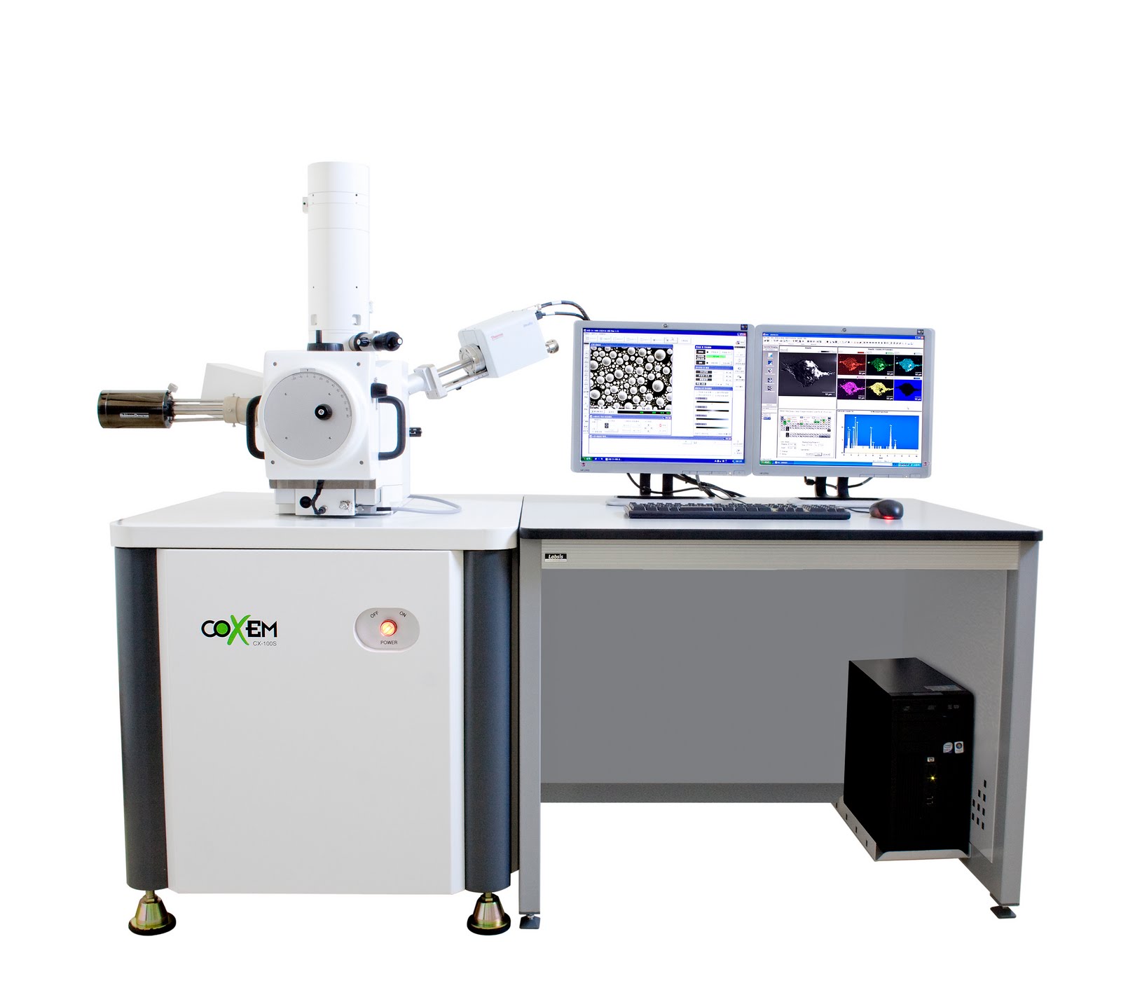
Scanning Electron Microscope, CX-100S
Versatile Tool to Access the Nano-World
The optical microscope is the most commonly used tool in surface metrology generally and it is widely used in educational programs, R&D and quality control. However, the optical microscope can not fulfill the growing demand for higher magnification due to its physical limitations. The CX-100S SEM is a powerful tool for surface characterization which produces high quality images with nano-scale resolution. Its software is using the graphical user interface and based-on and Microsoft Windows XP or 7. Company website: www.coxem.com
Indispensable Tool for Materials Analysis
CX-100S is an indispensable tool for various application areas in materials analysis. It has a high resolution (3.5 nm at 30 kV acceleration voltage and SE detector) and a high magnification imaging for surface morphology in the nanoscale. The clean imaging is due to its long depth of focus.
User Friendly Operation
NanostationTM is the powerful software for the system control and image analysis for the CX-100S SEM. It is designed and based-on Microsoft Windows XP and adapted a user-friendly interface. NanostationTM allows for a customized toolbars for repeat job setup.
High Performance / Economic Grade
The CX-100S is a state-of-the-art SEM with a veriety of detector choices, the user can enjoy a high performance SEM at an economic price.
Rapid Analysis
The CX-100S uses an oil-free turbo molecular pump. The speed of the pump will allow for imaging in under five minutes up to 10-6 torr.
Diverse Range of Applications
CX-100S provides the best imaging solution over a wide spectrum of samples from bio-molecules to metal samples. The CX-100S can be equipped with additional detectors like EDS and/or BSE and can run both simultaneously.
Contact: sem.jeong@gmail.com
피드 구독하기:
덧글 (Atom)